For going in to more details, take a look of notations that are used in this blog.
1] tc2q – clock to q of filp-flop 2] ts / tsetup – setup time
3] th/ thold – hold time 4] tpd – combinational delay
5] Data path – DP 6] Clock path – CP
And few are the definitions wrt the clock and DFF parameters

setup time – min. time D should present stable before active clock edge.
hold time – min. time D should present stable after active clock edge.
clk2q time – min time required to transfer changes at the output after active edge of clk.
There are certain conditions for violation free circuit.
The min and max value of combinational delay without timing violations
1] clock period >= tsetup + thold timing violations
2] min delay of combn > thold if not hold violations
3] max delay of combn < clock period – ts if not setup violations
find the max frequency from given specification
max freq = 1/ min(period)
case 1 when single value of delay specified
min(period) = tc2q + tpd + ts ;
case 2 when (min,max) delay specified
min(period) = max(DP) – min(CP) + ts ;
find the circuit has any setup , hold violations
1>>for setup violation check
step 1 , find the max(DP), and min(CP)
let td = max(DP)
step 2, tclk = clock period +min(CP) – tsetup
setup slack = tclk – td > 0 means no setup violations else it is
2>>for hold violation check
step 1 , find the max(CP) and min(DP)
let td = min(DP)
step 2, tclk = mam(CP) + thold
setup slack = td – tclk > 0 means no hold violations else it is
ex1. find the max frequency of design below
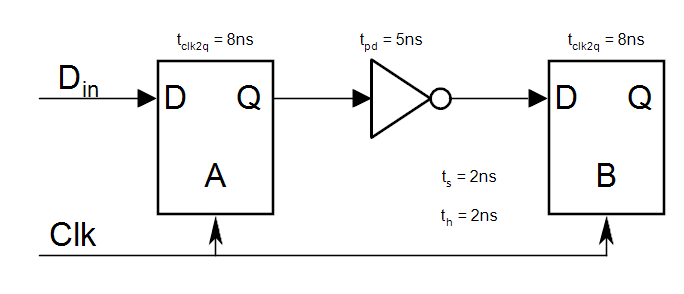
min(period) = tc2q + tpd + ts
= 8+5+2 = 15ns
frequency = 1/15 ns = 66.6667MHz
ex2. find the max frequency of design below
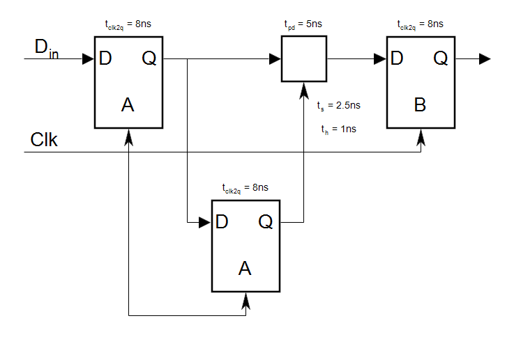
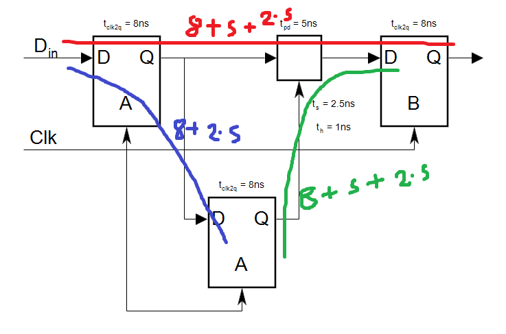
min(period) = tc2q + tpd + ts = 8+5+2.5 = 15.5ns . frequency = 1/15.5 ns = 64.5161MHz
ex3. find the max frequency of design below with min max specification
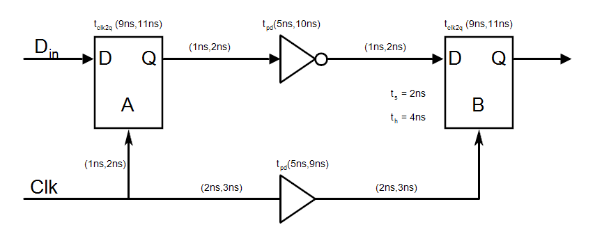
case 2 when (min,max) delay specified
min(period) = max(DP) – min(CP) + ts ;
max(DP) = 2+11+2+10+2 = 27ns
min(CP) = 2+5+2 = 9ns
min(period) = 27 – 9 + 2 = 20ns
frequency = 1/20ns = 50Mhz
Some more examples
For Violation Free Circuit:
Clock period > setup time + hold time
Min delay of combinational path > hold time of capture FF
Max delay of combinational path < clock period – setup time of capture FF
Example.1
| Specification of FF circuit | |||||
| Setup | Hold | Clock Period | Tclk2q delay | Net Delay | Combi Logic Delay |
| 2ns | 1ns | 10ns | 0ns(ideal) | 0ns(ideal) | 0.5ns |
0.5ns > 1ns hold violation
0.5ns < 10-2ns = 8ns no setup violation
Example.2
| Specification of FF circuit | |||||
| Setup | Hold | Clock Period | Tclk2q delay | Net Delay | Combi Logic Delay |
| 6ns | 5ns | 10ns | 0ns(ideal) | 0ns(ideal) | 0.5ns |
0.5ns > 5ns hold violation
0.5ns < 10-6ns = 4ns no setup violation
Example.3
| Specification of FF circuit | |||||
| Setup | Hold | Clock Period | Tclk2q delay | Net Delay | Combi Logic Delay |
| 3ns | 2ns | 10ns | 0ns(ideal) | 0ns(ideal) | 5ns cant be farther reduced |
5ns > 2ns no hold violation
5ns < 10ns – 3ns = 7ns no setup violation
Example.4
| Specification of FF circuit | |||||
| Setup | Hold | Clock Period | Tclk2q delay | Net Delay | Combi Logic Delay |
| 4ns | 3ns | 10ns | 0ns(ideal) | 0ns(ideal) | 8ns cant be farther reduced |
8ns > 3ns no hold violation
8ns < 10ns – 4ns = 6ns setup violation
For Violation Free Circuit: With T_capture and T_launch
Clock period > setup time + hold time [clock condition]
Min delay of combinational path > (T_capture – T_launch ) + hold time [min delay/Hold condition]
Max delay of combinational path < clock period +(T_capture – T_launch ) – setup time [max delay/setup condition]
Example.5
| Specification of FF circuit | |||||
| Setup | Hold | Clock Period | Tclk2q delay | Net Delay | Combi Logic Delay |
| 3ns | 2ns | 10ns | 0ns(ideal) | 0ns(ideal) | 11ns cant be further reduced |
Clock period > setup time + hold time
10ns > 3ns + 2ns clock period condition is satisfied
Min combinational delay > hold time
11 ns > 2ns no hold violation
Min combinational delay < clock period – setup time
11ns < 10 ns – 3 ns = 7ns setup violation here
T_ capture/ T_ launch delay between clk and capture / launch FF
11ns < 10ns + (t_c – t_l) – 3ns
4ns < t_c – t_l ignore the T_launch = 0ns prefer to change T_capture = 5ns
11ns < 10ns + 5ns – 3ns , 11ns < 12 ns so no setup violation here
Again check for hold condition
11ns > (t_c – t_l) + 2 ns ; 11 ns > 7ns still it is not violate the hold condition
Example.6
| Specification of FF circuit | |||||
| Setup | Hold | Clock Period | Tclk2q delay | Net Delay | Combi Logic Delay |
| 3ns | 5ns | 10ns | 0ns(ideal) | 0ns(ideal) | 2ns cant be further reduced cant inc the combi delay |
Clock period > setup time + hold time
10ns > 3ns + 5ns = 8ns clock period condition is satisfied
Min combinational delay < clock period – setup time
2ns < 10 ns – 3 ns = 7ns no setup violation here
Min combinational delay > hold time
2 ns > 5ns hold violation
2ns > 5ns + (t_c – t_l)
-3ns > (t_c – t_l)
T_ capture/ T_ launch delay between clk and capture / launch FF
ignore the T_ capture = 0ns prefer to change T_ launch = 4ns
2ns > 5ns + 0 – 4ns , 2ns > 1ns so no hold violation here
T_ capture – T_ launch know as clock skew
Example.7
| Specification of FF circuit | |||||
| Setup | Hold | Clock Period | Tclk2q delay | Net Delay | Combi Logic Delay |
| 6ns | 5ns | 10ns | 0ns(ideal) | 0ns(ideal) | 0.5ns |
Clock period > setup time + hold time
10ns > 6ns + 5ns = 11ns clock period condition is not satisfied
Max combinational delay < clock period – setup time
0.5ns < 10 ns – 6 ns = 7ns no setup violation here
Min combinational delay > hold time
0.5 ns > 5ns hold violation
Clock period > setup time + hold time [clock condition]
Min delay of combinational path > (T_capture – T_launch ) + hold time [prefer T_launch ]
Max delay of combinational path < clock period +(T_capture – T_launch ) – setup time [prefer T_capture]
With different terminology some examples with clock skew
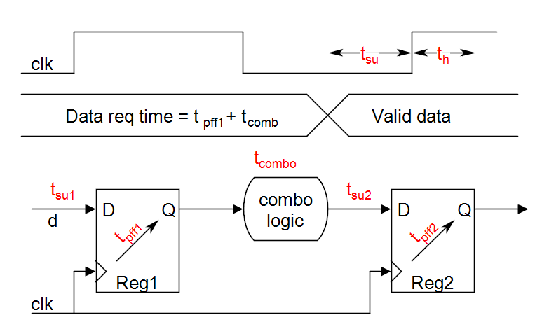 To find the maximum operating frequency for the design, find out the data required time and data arrival time. The data required time is the addition of all the delays in the register-to-register path. where Tclk is the one clock cycle
data required time = tpff1 + tcomb
data arrival time = Tclk – tsu2,
maximum frequency > data required time = data arrival time
tpff1 + tcomb = Tclk – tsu2
tpff1 + tcomb + tsu2 = Tclk
Freq. = 1/[tpff1 + tcomb + tsu2 ]
for values tpff1 =4ns tcomb =2ns tsu2 = 4ns
Freq = 1/[4+2+4]ns = 100Mhz
Skew in Design
When launch flip-flop is triggered first and capture flip-flop is triggered last, there is skew in the clock pulse and it is called as positive clock skew. Clock and data travels in the same direction and due to buffer delay the clk1 is delayed by delay of buffer as compared to clk input of register Reg1.
data required time = tpff1 + tcomb
data arrival time = Tclk – tsu2 + tbuf
maximum frequency > data required time = data arrival time
tpff1 + tcomb = Tclk – tsu2 + tbuf
tpff1 + tcomb + tsu2 – tbuf= Tclk
Freq. = 1/[tpff1 + tcomb + tsu2 – tbuf]
for values tpff1 =4ns tcomb =2ns tsu2 = 4ns, tbuf = 2ns
Freq = 1/[4+2+4 – 2]ns = 125Mhz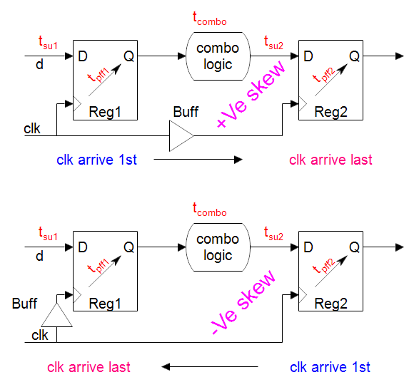 when source flip-flop is triggered last and destination flip-flop is triggered first. In the other way one can perceive that the clock and data are traveling in the opposite direction. Called negative skew design.
To find the maximum operating frequency
data required time = data arrival time.
data required time = tpff1 + tcomb + tbuf
data arrival time = Tclk – tsu2,
tpff1+tcomb+ tbuf = Tclk-tsu2
Tclk= tpff1+tcomb+ tsu2 + tbuf
Fmax= 1/( tpff1+tcomb+ tsu2 + tbuf)
for values tpff1 =4ns tcomb =2ns tsu2 = 4ns, tbuf = 2ns
Freq = 1/[4+2+4 + 2]ns = 83.3 MHz
Clear that negative clock skew degrades the performance of design
Please let me know, any one has any quires.