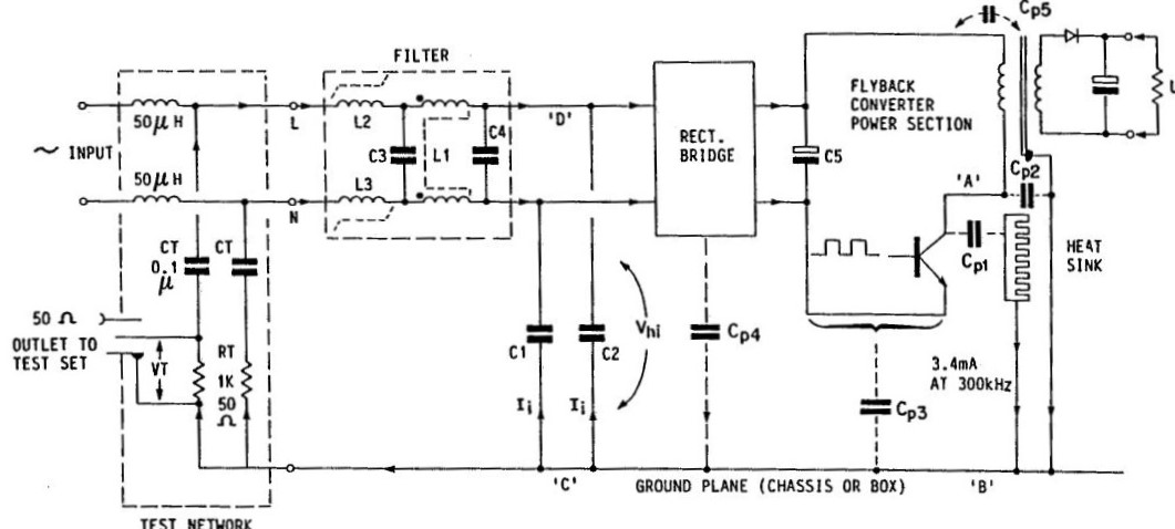
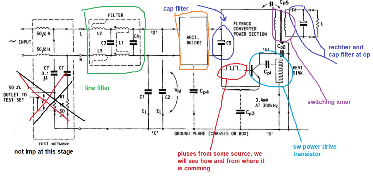
Hi, in this article, some of the 12 and 5 voltage smps circuit we will see and what common among them and what basic we can learn. We try to get basic block diagram of smps then we make partitions to that block diagram along with circuit that make it.
Generally you will get this kind of block diagram for the smps, lets make some paint work on it to make alignment to our brain to digest it.
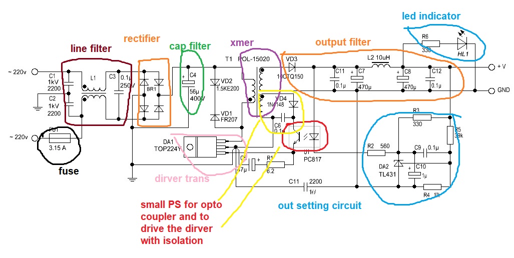
From the paint work it is seen that smps has or start with line filter – rectifier bridge – capacito filter – switching transformer – output rectifier – output capacitor filter , along with this there is transformer drive which is driven by pulses and it should have some heat sink to cool for the more reliable over the duration of operation, i guess.
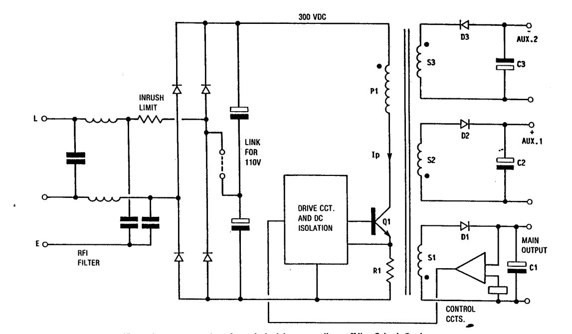
Lets see one more refine block diagram ,
Yahh, it has link for 110v supply support, it would be better to have a fuse in series with line, and MOC for the protect across it, any way we see these in coming circuits. We can notes we can have multiple output if needed also a feed back path also taken from output stage which control the drive stage, that’s nice.
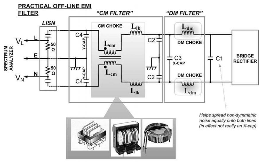
how line filter looks like,
hope you got it, definitely you saw these kind of stuff some where,
so we start taking circuits one by one and make paint work on it to understand or align with basic block diagram.
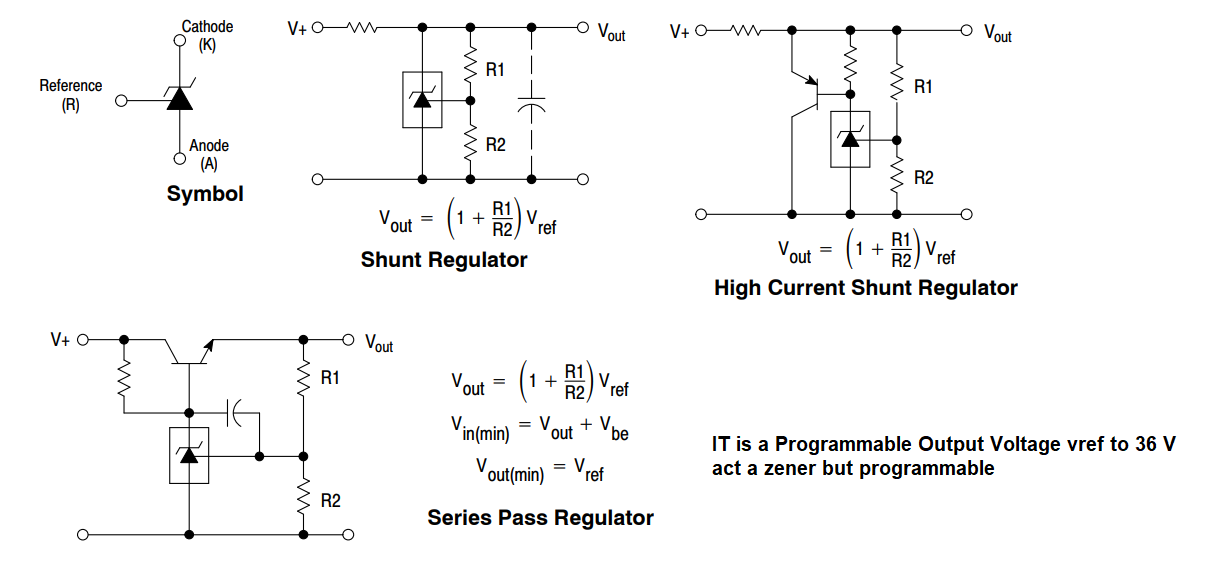
before it take a quick look TL431 item, from its datasheet, it seems Zener with programmable voltage setting.
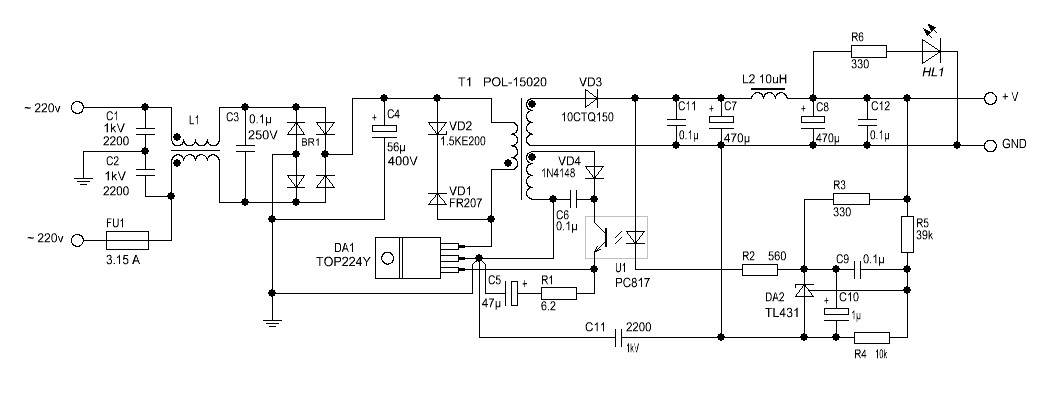
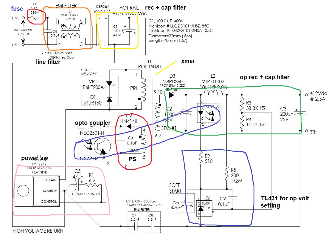
Below circuit now petty much looks like what we expect, lets start paint work on it.
SO this circuit has fuse and additional led power indicator and pi type output filter, the output voltage is set thro tl431 using R5 andR4.
2] Moving to next circuit, it is looking same circuit with some modification, lets do the paint job on it.
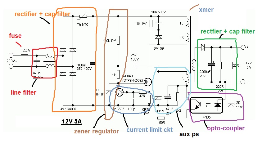
There are certain modification which results in low cost,
In place of tl431 here one zener is used for fix 12v output, a current limiting circuit setup is used for the protection of xmer, when current flow thro mosfet it will generate the voltage drop 0R22 resistor, and if high current flows the drop across exceed to the 0.7v and transistor switch on, which bring gate of mosfet to ground which make it off.
The next circuit is looking same as that before
, lets do the paint work on it,
Not seen any significant change or modifications with respective to earlier one.
Lets move to our next circuit, This circuit is also looks same with some small changes, Note here xmer is shown as ic symbol.
Lets do the paint work on it, for the partition of circuit items,
IT also looks same, with few changes, a npn and pnp combo used to make better sw to make mosfet off when over current thro R3 or when over voltage at the output happens.
In some circuits mosfet may replace with some chips, in our next circuit you can see that change, hope you follow what i seen,
 SO this circuit has fuse and additional led power indicator and pi type output filter, the output voltage is set thro tl431 using R5 andR4.
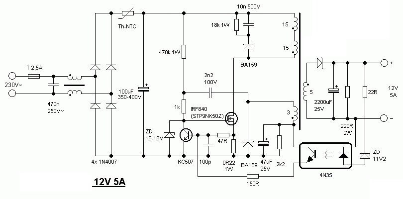
 There are certain modification which results in low cost,
 In place of tl431 here one zener is used for fix 12v output, a current limiting circuit setup is used for the protection of xmer, when current flow thro mosfet it will generate the voltage drop 0R22 resistor, and if high current flows the drop across exceed to the 0.7v and transistor switch on, which bring gate of mosfet to ground which make it off.
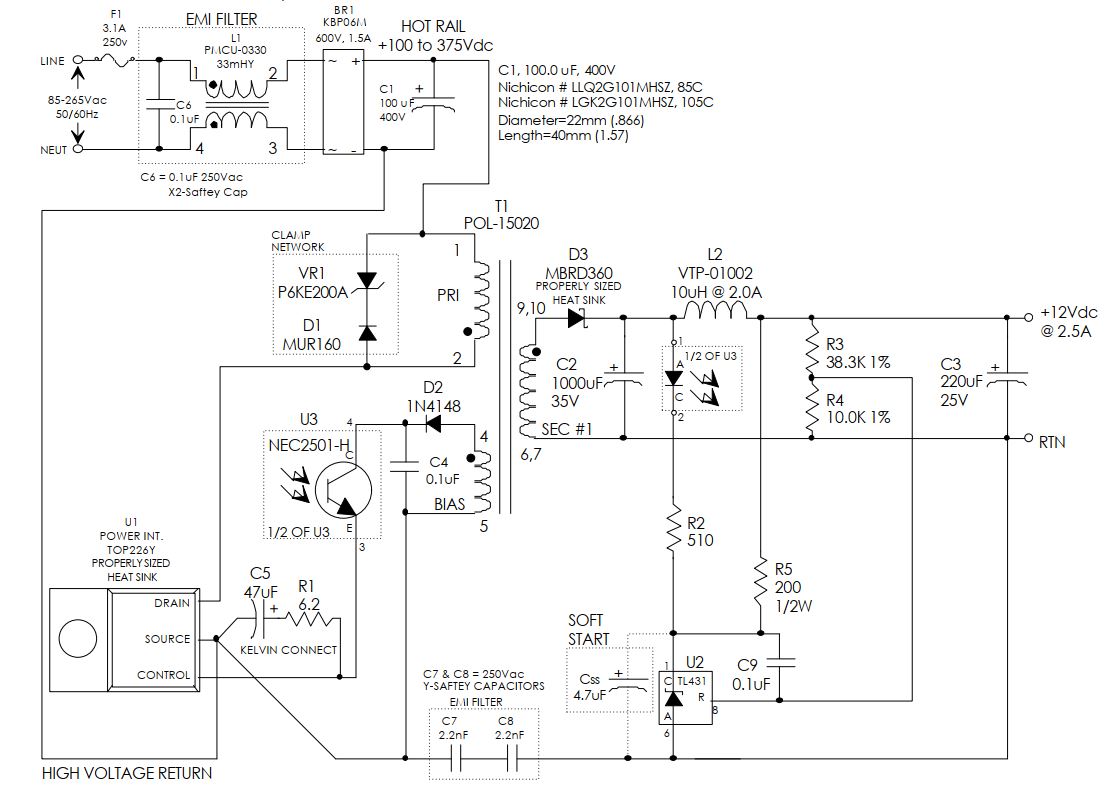
 Not seen any significant change or modifications with respective to earlier one.
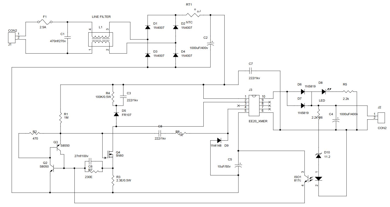 Lets do the paint work on it, for the partition of circuit items,
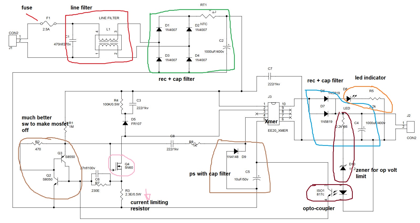 IT also looks same, with few changes, a npn and pnp combo used to make better sw to make mosfet off when over current thro R3 or when over voltage at the output happens.
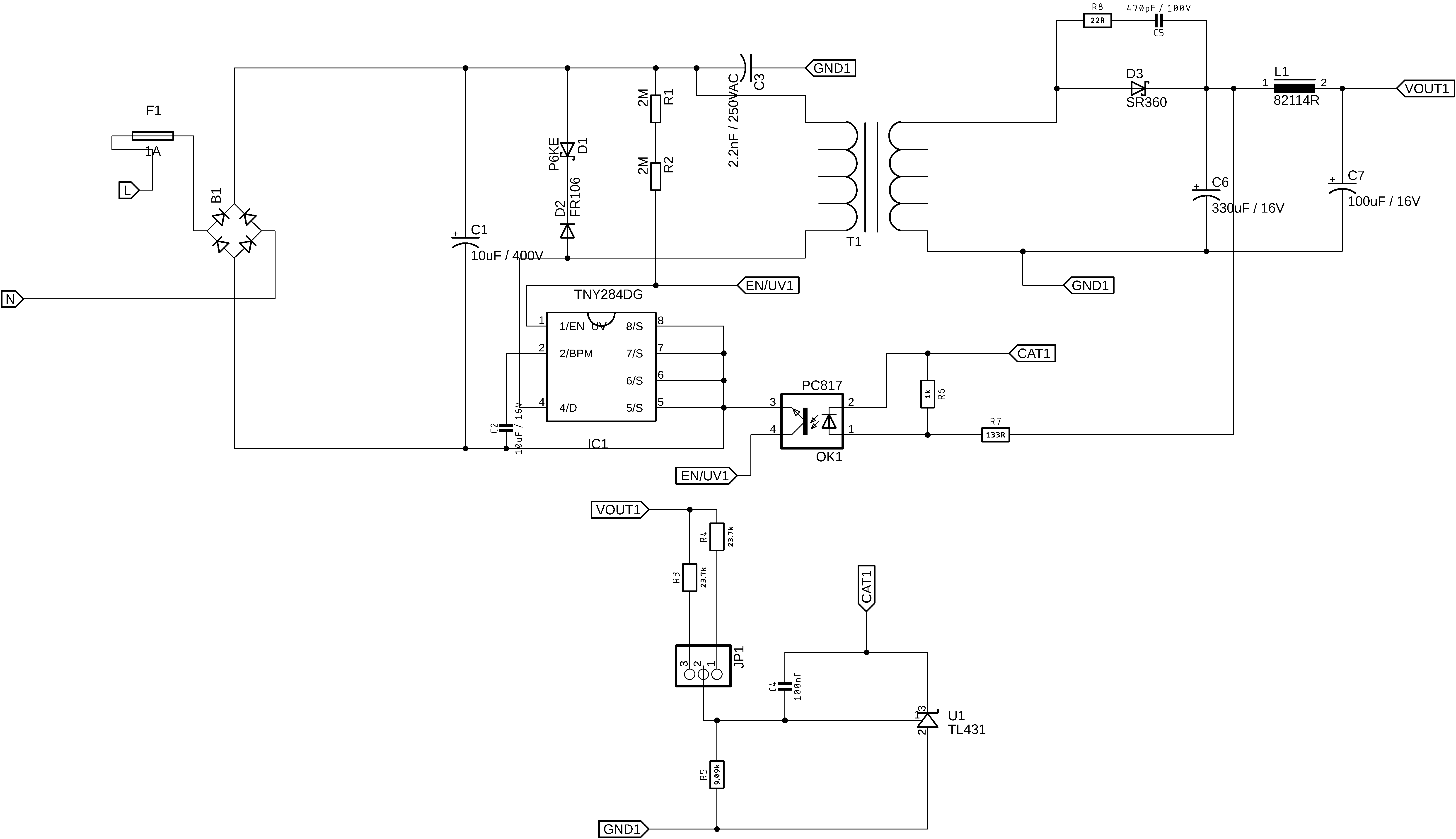 Comments are welcome